Posts

ET-3400 ROM - Program Test Video and Final Blog Post.

Resulting output from the program running on the ROM Replacement breadboard prototype with the patched ROM. Some characters in the alphabet are not possible to display on 7-segment displays, so you'll have to use your imagination a bit. Read the assembler listing in the previous post if you can't read it. While my RetroChallenge entry is complete, I still have to get PCBs manufactured and finish designing the adaptor PCB. Any further information on my progress will be posted on the groups.io/ET-3400 web site. Mark C.

ET-3400 ROM - Message Program Assembly

I intended to place this programming test in the new 8K ROM section of the ROM replacement board, however the program I was copying from (out of the ET-3400 Manual) was self-modifying and needed a rewrite so that it would run in ROM and use the RAM in the lower 512 bytes for variables. After I got into it I thought it would be relatively easy, but I was assuming that the 6800 CPU programming was similar to 6502 CPU programming since the 6502 was modelled on the 6800. However it turns out that was a false assumption, and my programming experience on the 6800 wasn't up to speed. The 6800 doesn't have indirect addressing mode and the program was self modifying so that it could do a sort-of indirect addressing. Also there were no opcodes to transfer the X register to the ACCA or ACCB register or the stack as far as I could tell. It was going to take me a lot longer to learn enough basic 6800 code to get this done in time, so I reverted to editing and extending the program in it'

ET-3400 ROM - Programming gains and losses

To write the program I wanted I was going to use ideas from the examples in the ET-3400 manual to help me create my little demo program. I also needed an assembler for 6800 code.  Turns out both of those tasks had already been mostly done previously and I had forgotten about them. I couldn't find a  suitable free assembler for Windows. I had used the Task Assembler (aka TASC) in DOS in the distant past for some Z80 code, and I think it could also assemble for different processors. Anyway that was so long ago and I couldn't spend the time looking for it. I also couldn't find a version of TASC on the www that I could access. All my Google searches pointed to CRASM which was for Linux and that rang a bell... I rebooted into my Ubuntu partition and it turns out that I had already installed CRASM probably last year and had forgotten about it. Good, one down, next... I was looking through the ET-3400 example programs and it turns out that Example 4 on page 61-62 was virtually w

ET-3400 ROM - DRAFT Gerber files, Schematic and Description sheet uploaded.

Image
I created the draft version of the gerber files, the schematic and a description sheet for the board. Unfortunately, once again, I have to discuss panelisation and v-cuts with JLCPCB before I place an order as I am not sure which option to choose so I get the right outcome. I want to make sure the artificial notch in the PCB is drilled between two boards layed out end to end (see below image). If the boards were in the same orientation, the centre notch is not round any more and is impossible to drill. I eventually got this right on my last order with them but it took days to explain. Hopefully things will go smoother this time. I also updated the Programming adapter PCB a bit more to clean it up. I'm never 100% satisfied with the PCB artwork and have to keep fiddling with it until it's perfect and it never is. The longer I leave it the more I modify it. I worked out I need pogo pins about 11-13mm high above the PCB that will compress down to about 10mm, if there is such a thin

ET-3400 ROM - Programming Adaptor

Image
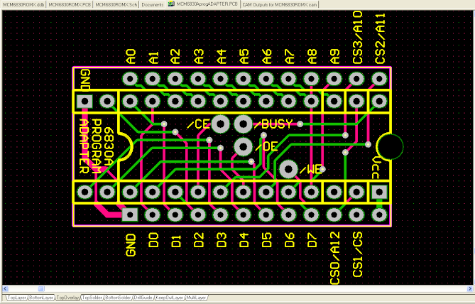
Thinking that it would be far more convenient to have a programming adaptor to program the SMD EEPROM after it was installed, rather than once off before it was installed I kept worrying had I allowed adequate space to design one at a later stage after this project was completed. I thought that with a bit of time up my sleeve before the end of the RetroChallenge I'd like to be sure that it was do-able and that I wasn't going to make something that was difficult or impossible to reprogram. I decided to start a PCB layout for a programming adaptor just to see if it was going to work. That was 2 days ago, and I realised that one of the pads that I had for the extra 4 pins was not in the best location, so I decided to spend some time in moving the pad to make the design of the adaptor workable. At first I was only going to do part of the layout, but once I got into it the retro  adrenaline  kicked in and I could see that it wasn't too difficult to finish it off. So now I have v

ET-3400 ROM - PCB-3D and Gerber preview

Image
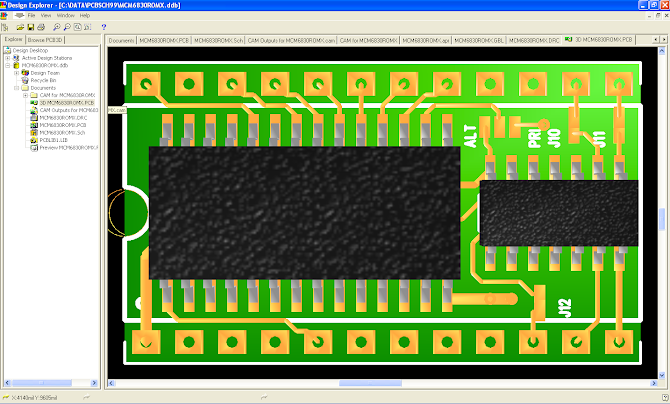
 I completed the artwork checks (PCB artwork vs. Schematic) and glad I did. There were a few minor errors, mainly to do with component designators and sequence for R10, R11 and R12 which were labelled different on my cct diagram vs. the PCB artwork. I still have to make some minor adjustments but it was close enough for this update.  I generated the 3D board view in my PCB app. It's pretty crude compared to a lot of newer apps, but good enough for a rough idea. I also generated the gerber files and uploaded them to JLCPCB, but that was mainly so I could get a better image of the two sides of the PCB than my PCB app can display. The image below from JLCPCB site still has the errors I mentioned above. I haven't decided on colour choice yet, but in keeping with the unusual (for the time) white colour used on the solder mask on the original ET-3400 and the later model ET-3400A, I think white mask would do it justice. On my previous ROM Replacement project I had a lot of trouble exp

ET-3400 ROM - Draft PCB layout

Image
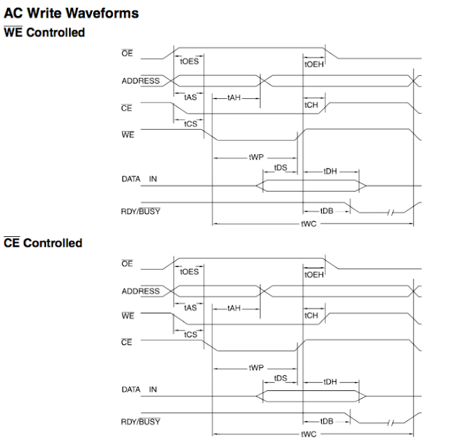
I checked the data sheet for the AT28C64 and there are some write waveforms shown as below. If I want to ever have a chance of making a programming adapter board then certain pins in the original circuit have to be disconnected from a permanent connection that I had for a read only operation. The 4 pins that need to be accessible to the EPROM programmer are /CE, /OE, RDY/BUSY, and /WE. I had forgotten /OE previously. So these pins need a way to be disconnected from their read circuit. The rest of the pins needed are accessible on the edges on the 24-pin socket. I'll probably be using SIL machine pins as the ROM pins to plug this into the ET-3400 motherboard. As can be seen in the above waveforms, an EPROM programmer could write to the EEPROM in a couple of ways, and both involve setting /WE, /CE and /OE high or low during the write cycle. If they are tied high or low in my original read only setup then the programmer could be damaged and it's unlikely that the EEPROM could be w