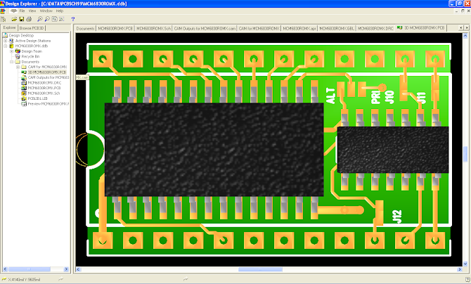
ET-3400 ROM - PCB-3D and Gerber preview
I completed the artwork checks (PCB artwork vs. Schematic) and glad I did. There were a few minor errors, mainly to do with component designators and sequence for R10, R11 and R12 which were labelled different on my cct diagram vs. the PCB artwork. I still have to make some minor adjustments but it was close enough for this update.
I generated the 3D board view in my PCB app. It's pretty crude compared to a lot of newer apps, but good enough for a rough idea.
I haven't decided on colour choice yet, but in keeping with the unusual (for the time) white colour used on the solder mask on the original ET-3400 and the later model ET-3400A, I think white mask would do it justice.
On my previous ROM Replacement project I had a lot of trouble explaining the notch on one end of the PCB which I insist in keeping (It's the best way I know to ensure the board is plugged in correctly and it looks a lot like a stock IC shaped notch). I wanted them to panellise it and rotate one half of the boards so that the notch was in the middle as a full round hole that they could drill. You'd think that would be simple enough to explain, but it took 3 days to explain via email and also via chat so I won't be going down that path again.
This time I think I'll panellise it myself with two boards opposite each other so that the two notches are on opposite sides and will line up in the centre. Hopefully then I can get them processed more easily and not have to explain it all over again.
I just need to fix up the few minor errors and next update should have the gerber files done. I've never used github and don't have an account, but that seems to be the place to go for this type of project. Alternatively I can more easily upload the schematics and the gerber files to the ET-3400@groups.io Files/Projects area (https://groups.io/g/ET-3400/files/5.%20Projects) and I think that would be more appropriate.


Comments
Post a Comment