ET-3400 ROM - Schematic Draft
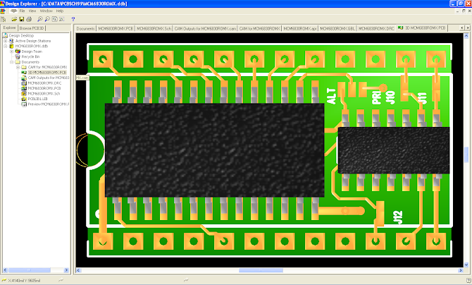
I've done the schematic quickly in Design Explorer 99SE running under virtual Windows XP. This is an old program but free and it works on my old MacBook.
The CS/CE logic needs to take the four CSx inputs into the original mask ROM and create a single active low /CE output to the EEPROM.
In logic terms we need a logic 0 out only when (CS0 = 1) AND (CS1 = 0) AND (CS2 = 1) AND (CS3 = 1). For any other combination of inputs we need a logic 1 out so that the EEPROM is NOT selected.
Since 3 of the 4 signals (CS0, CS2 and CS3) are normally active high we could push them through a 3-input NAND gate (74LS10) that will only go low out when all inputs are high. but we still have to deal with the CS1 input which is active low, so we'd have to mix the output of the 3-input NAND gate by pushing that through a 2-input NOR gate with the CS1 signal to create an active high out of that, then invert that again to create an active low. That would involve at least 2 TTL ICs and will make the PCB layout a tighter fit or too big.
We can do better than that if we first invert the active low CS1 signal and make it active high like the other three CS signals, then push all of those through a 4-input NAND gate (74LS20) to create an active low output which is what we need for our EEPROM /CE input. To invert the CS1 input we can use the spare 4-input NAND gate in the 74LS20 by connecting all the inputs together.
There are loading limits on driving TTL chips and typically a 74LS TTL output can only drive two 74LS TTL inputs, so if we tied all four inputs we'd be breaking that design rule and it may not work. Instead we can simple tie 3 of the 4 inputs high and put the CS1 signal into the other pin and that will produce the same resulting output without affecting the TTL loading. With this solution we only need one 14-pin TTL logic chip to help with the decoding.

I just noticed that I have D5 listed twice on the data bus exit to the AT28C64B EEPROM. Obviously the top one should be D4. I'll fix that later.
ReplyDeleteJust found another error while building the prototype. A0 on the ROM socket should be pin 24, not pin 12 as shown.
ReplyDelete