Posts

Showing posts from October, 2021

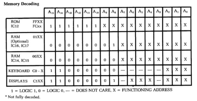
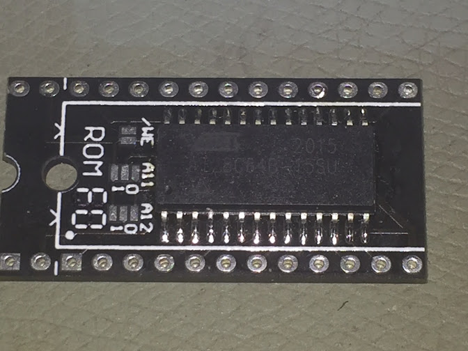
ET-3400 ROM - Program Test Video and Final Blog Post.

Resulting output from the program running on the ROM Replacement breadboard prototype with the patched ROM. Some characters in the alphabet are not possible to display on 7-segment displays, so you'll have to use your imagination a bit. Read the assembler listing in the previous post if you can't read it. While my RetroChallenge entry is complete, I still have to get PCBs manufactured and finish designing the adaptor PCB. Any further information on my progress will be posted on the groups.io/ET-3400 web site. Mark C.

ET-3400 ROM - Message Program Assembly

I intended to place this programming test in the new 8K ROM section of the ROM replacement board, however the program I was copying from (out of the ET-3400 Manual) was self-modifying and needed a rewrite so that it would run in ROM and use the RAM in the lower 512 bytes for variables. After I got into it I thought it would be relatively easy, but I was assuming that the 6800 CPU programming was similar to 6502 CPU programming since the 6502 was modelled on the 6800. However it turns out that was a false assumption, and my programming experience on the 6800 wasn't up to speed. The 6800 doesn't have indirect addressing mode and the program was self modifying so that it could do a sort-of indirect addressing. Also there were no opcodes to transfer the X register to the ACCA or ACCB register or the stack as far as I could tell. It was going to take me a lot longer to learn enough basic 6800 code to get this done in time, so I reverted to editing and extending the program in it'

ET-3400 ROM - Programming gains and losses

To write the program I wanted I was going to use ideas from the examples in the ET-3400 manual to help me create my little demo program. I also needed an assembler for 6800 code.  Turns out both of those tasks had already been mostly done previously and I had forgotten about them. I couldn't find a  suitable free assembler for Windows. I had used the Task Assembler (aka TASC) in DOS in the distant past for some Z80 code, and I think it could also assemble for different processors. Anyway that was so long ago and I couldn't spend the time looking for it. I also couldn't find a version of TASC on the www that I could access. All my Google searches pointed to CRASM which was for Linux and that rang a bell... I rebooted into my Ubuntu partition and it turns out that I had already installed CRASM probably last year and had forgotten about it. Good, one down, next... I was looking through the ET-3400 example programs and it turns out that Example 4 on page 61-62 was virtually w

ET-3400 ROM - DRAFT Gerber files, Schematic and Description sheet uploaded.

Image
I created the draft version of the gerber files, the schematic and a description sheet for the board. Unfortunately, once again, I have to discuss panelisation and v-cuts with JLCPCB before I place an order as I am not sure which option to choose so I get the right outcome. I want to make sure the artificial notch in the PCB is drilled between two boards layed out end to end (see below image). If the boards were in the same orientation, the centre notch is not round any more and is impossible to drill. I eventually got this right on my last order with them but it took days to explain. Hopefully things will go smoother this time. I also updated the Programming adapter PCB a bit more to clean it up. I'm never 100% satisfied with the PCB artwork and have to keep fiddling with it until it's perfect and it never is. The longer I leave it the more I modify it. I worked out I need pogo pins about 11-13mm high above the PCB that will compress down to about 10mm, if there is such a thin

ET-3400 ROM - Programming Adaptor

Image
Thinking that it would be far more convenient to have a programming adaptor to program the SMD EEPROM after it was installed, rather than once off before it was installed I kept worrying had I allowed adequate space to design one at a later stage after this project was completed. I thought that with a bit of time up my sleeve before the end of the RetroChallenge I'd like to be sure that it was do-able and that I wasn't going to make something that was difficult or impossible to reprogram. I decided to start a PCB layout for a programming adaptor just to see if it was going to work. That was 2 days ago, and I realised that one of the pads that I had for the extra 4 pins was not in the best location, so I decided to spend some time in moving the pad to make the design of the adaptor workable. At first I was only going to do part of the layout, but once I got into it the retro  adrenaline  kicked in and I could see that it wasn't too difficult to finish it off. So now I have v

ET-3400 ROM - PCB-3D and Gerber preview

Image
 I completed the artwork checks (PCB artwork vs. Schematic) and glad I did. There were a few minor errors, mainly to do with component designators and sequence for R10, R11 and R12 which were labelled different on my cct diagram vs. the PCB artwork. I still have to make some minor adjustments but it was close enough for this update.  I generated the 3D board view in my PCB app. It's pretty crude compared to a lot of newer apps, but good enough for a rough idea. I also generated the gerber files and uploaded them to JLCPCB, but that was mainly so I could get a better image of the two sides of the PCB than my PCB app can display. The image below from JLCPCB site still has the errors I mentioned above. I haven't decided on colour choice yet, but in keeping with the unusual (for the time) white colour used on the solder mask on the original ET-3400 and the later model ET-3400A, I think white mask would do it justice. On my previous ROM Replacement project I had a lot of trouble exp

ET-3400 ROM - Draft PCB layout

Image
I checked the data sheet for the AT28C64 and there are some write waveforms shown as below. If I want to ever have a chance of making a programming adapter board then certain pins in the original circuit have to be disconnected from a permanent connection that I had for a read only operation. The 4 pins that need to be accessible to the EPROM programmer are /CE, /OE, RDY/BUSY, and /WE. I had forgotten /OE previously. So these pins need a way to be disconnected from their read circuit. The rest of the pins needed are accessible on the edges on the 24-pin socket. I'll probably be using SIL machine pins as the ROM pins to plug this into the ET-3400 motherboard. As can be seen in the above waveforms, an EPROM programmer could write to the EEPROM in a couple of ways, and both involve setting /WE, /CE and /OE high or low during the write cycle. If they are tied high or low in my original read only setup then the programmer could be damaged and it's unlikely that the EEPROM could be w

ET-3400 ROM - Almost there

Didn't get a lot done today. I did manage to finish off adding R10, R11 and R12 and have added the jumper pads for J10, J11 and J12 as well as the PRI/ALT pads completed. So that extra feature is completed. They are all accessible on the top of the PCB. But,  I should also add pads for the /CE pin too just in case I find that I need to isolate it later. There's not much room left on the top so that may be on the underside. Also I am going to try and route those extra programming pins (RDY/BUSY, /WE and /CE) out somewhere accessible so a wire can be soldered onto them, or some similar trick for programming. These may also have to be routed on the underside to one edge. Whatever I do, I won't be adding more layers, two layers and vias will have to do it or bust.

ET-3400 ROM - Circuit changes and more tests

Image
To test the new feature I needed to modify the circuit so I could choose 1K or 8K setup. The changes to the circuit are shown below. Remembering that /CS1 input is active from $E000..$FFFF, I passed CS3/A10 and CS2/A11 through to the EEPROM and added J10, J11 and J12 which are used to modify the /OE signal so it's only active for a lower range of addresses. For example if all 3 jumpers are fitted, then the /OE will only be active when all 3 are high which would be from address $FC00..$FFFF (1K). If all 3 are left open then the 3 pull-up resistors R10, R11 and R12 along with the /CS1 input signal will enable /OE for the whole 8K from $E000..$FFFF (8K). That also means CS0/A12 would need to be passed through to A12 on the EEPROM and the PRI jumper would allow that to happen. That adds the extra feature I wanted, but to keep the original project goal (and not move the goal posts) I still need to have A12 on the EEPROM side be either high or low regardless of A12 input, and the EEPROM

ET-3400 ROM - Feature Creep

Image
I got  most of the PCB artwork done in accordance with my original plan, and then I thought perhaps I could add an extra feature that I hadn't planned originally. At the moment I have an 8K EEPROM and using one of two 1K banks selectable by a jumper. I am wasting 6K out of the 8K. I had a look at the memory map for the ET-3400 and it seems that there is no memory use between $C200 and $FBFF below the monitor ROM. Also the add-on ETA-3400 Memory I/O Accessory unit doesn't make use of any of that space. The other project I am working on (that big mess of breadboards and wires in my earlier pictures) is a Memory I/O Accessory unit that does use all of that space, but not everyone will have that configuration and may only have the stock ET-3400 unit or the stock Memory I/O unit. There is sufficient space in this EEPROM to have 8K of ROM from $E000..$FFFF if you don't need to have two ROM versions. Wouldn't it be nice to be able to configure the board to make use of that spa

ET-3400 ROM - SO what ?

Image
In order to speed up the PCB layout process, I have copied another PCB layout I used for a similar ROM replacement PCB. This new project also has an SOIC-14 that the other one didn't. I've only used SMD components a few times so far and the PCB application has numerous libraries that I am still struggling to find things in. I think some of the library entries are merged from an older version of the application I am using, so there are some custom ones mixed in there that I drew myself previously. It's a bit of a mess. I found the SOIC-28 footprint for the 28C64B on the last project and that was called SOL-28 so that one was OK to re-use, but now I need an SOIC-14 for the 74LS20 dual 4-input NAND gate. At least that's what the supplier states it is. The data sheets show slightly different naming, so I'm going to have to check the dimensions. I looked for a SOIC-14 in the library and find that there are a number of different but similar sounding and looking components

ET-3400 ROM - PCB layout planning

Image
The size of the PCB I am planning will be the same size as the original 24-pin DIP IC. Within that footprint I hope to fit an AT28C64B SOIC-28 EEPROM and a 74LS20 SOIC-14 TTL chip on one or both sides of the PCB. To show how tight that might be here is one that I am working on for an Apple II europlus ROM replacement that is nearly finished, although this one is 28pin DIP size with only the AT28C64B on the top and a small 5-pin 1-bit inverter on the back. Besides the EEPROM, I am aiming to put another chip on the top or bottom (if there isn't enough space). The orientation of the EEPROM on the PCB will affect the track routing quite a lot. Here is two possible plans that include the address lines A0..A9, data lines D0..D7, power +5V and GND, and some CS lines. I've sketched in where the pins on the socket would have to be routed to the EEPROM. The drawing is not to scale, just a rough layout to see which one works best. I always do my own routing manually. Auto-routing takes aw

ET-3400 ROM - testing /CE and /OE options

Image
The original ROM does not have a separate /OE and /CE pins, instead it puts data onto the database once the four CS pins meet the required conditions. This is not uncommon for ROMs of this vintage. We are using a modern replacement EEPROM and it has separate /CE (Chip Enable) and /OE (Output Enable) pins. I have seen various ways to use those pins in other memory expansion projects. Sometimes one pin is tied to GND and the other pin is used to enable the chip to output the data onto the bus. At other times both pins are tied together so that the both go low or high at the same time. This gives several options: Option 1. /CE tied low permanently and /OE set low to read data, then high to disable output. Option 2. /OE tied low permanently and /CE set low to read data, then high to disable output. Option 3. /CE and /OE tied together and both set low to read, or high to disable output. The data sheet shows the following Operating Modes: Going by this you would set /CE low and /OE low for r

ET-3400 ROM - Testing the circuit

Image
Now to test out the circuit. First thing I am going to check is to make sure my ET-3400 works normally before I remove the original MCM6830A mask ROM. It boots up and resets to ' CPU UP. ' on the display. I then examine a few memory locations and it's working normally. The ROM is removed and the new circuit on the breadboard is plugged into the ROM socket via the 24 pin ribbon cable. To reduce the chance of smoking up any ICs on the breadboard I removed the 28C64B EEPROM and the 74LS20, connected up my multimeter to Vcc and GND to check the +5V rail. Powered on and the +5V rail is good. I turned the backlight on my multimeter and it's a bit over exposed, but you can see 4.9444 if you squint. The ET-3400 display is showing ' 8.8.8.8.8.8. ' as it should, since there is no monitor ROM of any kind fitted to run any code. So it's just displaying whatever is in memory. I also checked the power and ground connection points for the ICs on the breadboard and they are

ET-3400 ROM - Programming the EEPROM

Image
Only a few months ago I needed a Universal programmer so I could program GALs and some newer/larger EPROMs that my old home made Electronics Australia 1993 EPROM programmer could not program. I was considering the popular TL866-II Plus that a lot of people are recommending due to the low cost. Some reviews stated that it had issues with programming certain brands of GALs so I was hesitant against purchasing one. While shopping for something more capable I was lucky enough to score this basic model Wellon VP-299 Universal Programmer on eBay for a low $50AU. Typically these are $250AU or more. Unfortunately it failed one week later after I had pushed it a bit hard with some known faulty EPROMs. Two months later I finally had it working again. The patched OUTCH monitor routine is shown listed below the programmer and I've circled the five bytes that need to be amended. These are for the address in ROM that the 1K is mapped to. The equivalent byte in the EEPROM will be whatever 1K bank

ET-3400 ROM - Editing the EEPROM firmware

Image
Before I can program the EEPROM with the two monitor versions I am planning to install I have to figure out where in the EEPROM memory each bank should go into. The EEPROM is 8KB in size and the monitor program is only 1KB in size. Address bits A0..A9 are used to select any address in the 1KB address range. i.e. 10 address bits = 2^10 bytes = 1024 bytes (1KB). Incoming Address line A10, A11 and A12 and CS are used as the address decoding bits to map the ROM into memory at $FC00..$FFFF. I am using EEPROM address lines A10, A11 and A12 to select which of the eight 1K banks possible in the EEPROM is selected by tying them hi or low. That gives us our 8 possible banks below: A12  A11  A10  EEPROM bank   EEPROM address range 0      0      0      0              $0000..$03FF 0     0    1    1            $0400..$07FF 0     1    0    2            $0800..$0BFF 0     1    1    3            $0C00..$0FFF   1    0    0    4            $1000..$13FF 1     0    1    5            $1400..$17FF 1     1   

ET-3400 ROM - Building the Prototype

Image
To build the prototype I can't easily use SMD components on a breadboard without appropriate adapters and I don't have any suitable ones. I have several 28C64B EEPROMs in SOIC-28 format that I purchased for another project and luckily I also have one in DIP-28 size. Since these are essentially the same part in different sizes I can use the DIP-28 EEPROM for testing the circuit. Also I don't have any 74LS20's in SMD size yet, but I can use a 74LS20 in DIP-14 size for the prototype. That solves the parts requirements, but unfortunately my ET-3400 has another in-progress breadboard project on it already and I don't want to pull it all apart yet as I haven't finished it. This shows how full my ET-3400 breadboard is already. You couldn't squeeze an ant in there. I decided to use an old Wish breadboard I have. The yellowing plastic on it qualifies it as a retro part by itself. It might be old, but it's a lot better than some of the garbage breadboards they mak

ET-3400 ROM - Schematic Draft

Image
I've done the schematic quickly in Design Explorer 99SE running under virtual Windows XP. This is an old program but free and it works on my old MacBook. The CS/CE logic needs to take the four CSx inputs into the original mask ROM and create a single active low /CE output to the EEPROM. In logic terms we need a logic 0 out only when (CS0 = 1) AND (CS1 = 0) AND (CS2 = 1) AND (CS3 = 1). For any other combination of inputs we need a logic 1 out so that the EEPROM is NOT selected. Since 3 of the 4 signals (CS0, CS2 and CS3) are normally active high we could push them through a 3-input NAND gate (74LS10) that will only go low out when all inputs are high. but we still have to deal with the CS1 input which is active low, so we'd have to mix the output of the 3-input NAND gate by pushing that through a 2-input NOR gate with the CS1 signal to create an active high out of that, then invert that again to create an active low. That would involve at least 2 TTL ICs and will make the PCB l

ET-3400 ROM - Selecting a suitable EPROM or EEPROM

Image
The original MCM6830A mask ROM is 1KB in size. the only EPROM I am aware of in 1KB size is the Intel 2708 EPROM and that is a hard to find part and awkward to program and operate because it requires +5V, -5V and +12V to operate and program. I happen to have two of them in my collection of EPROMs, one is installed in a DREAM 6802 I also own. I'm keeping them for that one day in the future I will be able to program them. While the ET-3400 does have those voltages on the main board, they are not available at the IC12 ROM socket, so I would have to have jumper wires or an on-board voltage generator to operate. Messy. Furthermore there are very few modern EPROM programmers that can program 2708's and I don't have one myself. Lastly it's only 1KB and I want to be able to choose from at least two ROM options so I need 2KB minimum. So I'm striking that off as a potential replacement. After that there is 2716 EPROM (2KB), 2732 EPROM (4K) in 24 pin size ICs, or a 2764 EPROM (

ET3400 ROM - Defining the problem

Image
 In order to come up with a potential solution for a replacement ROM, I first have to define the problem with the existing ROM. I found the following data on the original MCM6830A mask ROM. This image shows the physical connections to the ROM. This is straight out of the Heathkit ET-3400 Trainer manual page 112. Another piece of information I found shows the logical connection to the ROM. Notice that there are 4 Chip Select signals labelled CS0..CS3. This is quite unusual as most modern EPROMs or EEPROMs use only one CS pin. I'll have to take those extra CS pins into consideration in my design. The address, data and power pins are straight forward, but I also need to see how the CS pins are connected in circuit. This is an extract from the ET-3400 circuit diagram. From the circuit diagram we can see that CS0 is connected to address A12, CS1 is coming from IC2, CS2 is from address A11 and CS3 is from address A10. The monitor ROM resides in 1K of memory space from $FC00..$FFFF. Addre

RetroChallenge 2021 - ET-3400 ROM replacement

As this my first RetroChallenge entry I thought I'd start with a  relatively simple project. I've chosen to create a small ROM replacement board for an ET-3400 Microprocessor Trainer. As part of this project I am designing and drafting the schematic, testing the circuit design and creating PCB artwork ready for production. Background: The Heathkit ET-3400 Microprocessor trainer was sold as a kit or an assembled unit from about 1976. The trainer features a Hexadecimal keypad, 7-segment display, 500KHz 6800 CPU, 256 bytes of RAM, 1K Monitor ROM and a breadboard area for hardware experiments. more information on the unit can be found here: http://www.decodesystems.com/heathkit-et3400.html I purchased a second hand ET-3400 and a later model ET-3400A about 20 years ago and I've joined the ET-3400 group earlier this year -  https://groups.io/g/ET-3400 One of the problems with these early machines is that the ROMs are not pin compatible with modern JEDEC pinouts. In the case of th