ET-3400 ROM - Feature Creep
I got most of the PCB artwork done in accordance with my original plan, and then I thought perhaps I could add an extra feature that I hadn't planned originally.
At the moment I have an 8K EEPROM and using one of two 1K banks selectable by a jumper. I am wasting 6K out of the 8K.
I had a look at the memory map for the ET-3400 and it seems that there is no memory use between $C200 and $FBFF below the monitor ROM. Also the add-on ETA-3400 Memory I/O Accessory unit doesn't make use of any of that space.
The other project I am working on (that big mess of breadboards and wires in my earlier pictures) is a Memory I/O Accessory unit that does use all of that space, but not everyone will have that configuration and may only have the stock ET-3400 unit or the stock Memory I/O unit.
There is sufficient space in this EEPROM to have 8K of ROM from $E000..$FFFF if you don't need to have two ROM versions. Wouldn't it be nice to be able to configure the board to make use of that space, or have it as originally planned with two ROM versions. Then it would be up to the user to determine what configuration they wanted.
This is what is known as Feature Creep, where extra features are added part way through a project. Sometimes this can get in the way of finishing a project or getting away from the original intent, but I think I have plenty of time to at least consider it. If it doesn't look like it will work I can fall back to my original plan.
So now my project has two goals:
1. make a small PCB ROM replacement board with two selectable 1K ROM versions, and
2. allow for an alternate configuration where the top 8K of memory can be used as ROM.
First thing to consider is whether the /CS1 line from the motherboard will allow me to use the upper 8K because that's a show stopper otherwise.
Page 87 of the ET-3400 manual shows that IC12 is decoded by A15, A14, A13, A12, A11 and A10 (see table below). That places the ROM in 1K of space between $FC00 and $FFFF. The first three address lines A15..A13 are actually done on the motherboard by IC2 to produce the /CS1 signal which means any address from $E000..$FFFF (8K) is done on the motherboard. The extra address lines A12, A11 and A10 are the three signals decoded by the original mask ROM itself to bring the range down to $FC00..$FFFF (1K).
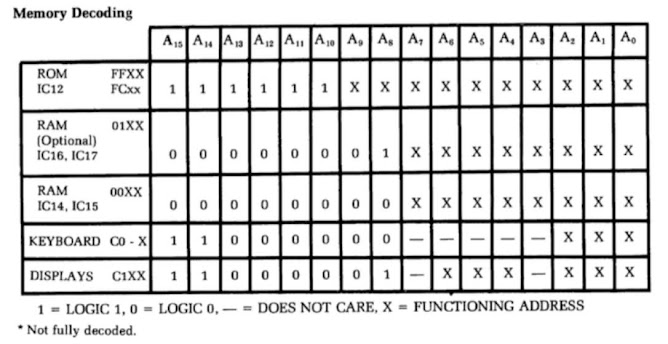
That's good news because it means if we ignore the 3 address lines from A12..A10 then the /CS1 signal will be active and can select any of the upper 8K memory space.
Show stopper avoided !
The tricky part will be trying to fit any changes in the remaining space and I haven't got a lot of real estate anyway.
Using my other ROM Replacement design I found that I needed to make the vias smaller on this design so I checked the PCB manufacturers web site (JLCPCB) to find out how small I could make them and I can go down to half the size of my previous design. This gives me more wriggle room.
Will there be enough room for the extra features, only trial and error will tell...
Comments
Post a Comment