ET-3400 ROM - PCB layout planning
The size of the PCB I am planning will be the same size as the original 24-pin DIP IC. Within that footprint I hope to fit an AT28C64B SOIC-28 EEPROM and a 74LS20 SOIC-14 TTL chip on one or both sides of the PCB.
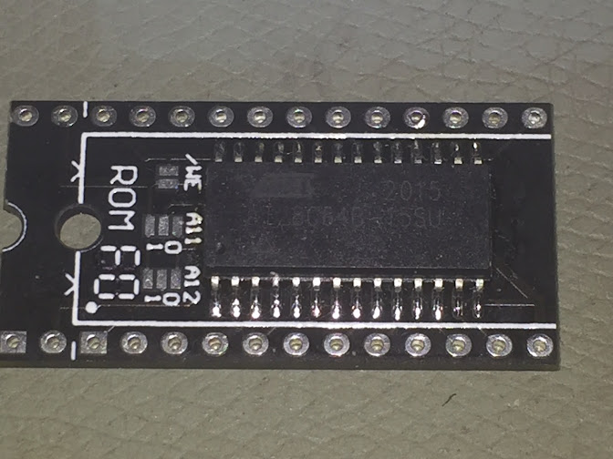
To show how tight that might be here is one that I am working on for an Apple II europlus ROM replacement that is nearly finished, although this one is 28pin DIP size with only the AT28C64B on the top and a small 5-pin 1-bit inverter on the back.
Besides the EEPROM, I am aiming to put another chip on the top or bottom (if there isn't enough space).
The orientation of the EEPROM on the PCB will affect the track routing quite a lot. Here is two possible plans that include the address lines A0..A9, data lines D0..D7, power +5V and GND, and some CS lines. I've sketched in where the pins on the socket would have to be routed to the EEPROM. The drawing is not to scale, just a rough layout to see which one works best.

I always do my own routing manually. Auto-routing takes away the fun and is never how you want it. There is a lot of prerequisites for auto-routing such as PCB footprints and complete circuits. I often start at the PCB layout for small circuits.
If you look at both options above it is clear that Plan A has a lot of the tracks crossing over each other and to the other side of the EEPROM, where Plan B has far less tracks crossing and is more straight forward. I haven't shown the 74LS20, but hopefully it will fit down below the EEPROM on the top side. I'll work that part out when I draw up the PCB in Design Explorer 99SE after I get all the above tracks in place.
In summary I am going with Plan b from Outer Space
if you flip the 'b' you can get a '9', good enough for 7-segment displays.
next I'll start drawing this up...
Comments
Post a Comment