ET3400 ROM - Defining the problem
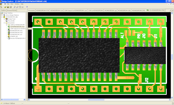
In order to come up with a potential solution for a replacement ROM, I first have to define the problem with the existing ROM.
I found the following data on the original MCM6830A mask ROM. This image shows the physical connections to the ROM. This is straight out of the Heathkit ET-3400 Trainer manual page 112.
Another piece of information I found shows the logical connection to the ROM. Notice that there are 4 Chip Select signals labelled CS0..CS3. This is quite unusual as most modern EPROMs or EEPROMs use only one CS pin. I'll have to take those extra CS pins into consideration in my design.
The address, data and power pins are straight forward, but I also need to see how the CS pins are connected in circuit. This is an extract from the ET-3400 circuit diagram.
From the circuit diagram we can see that CS0 is connected to address A12, CS1 is coming from IC2, CS2 is from address A11 and CS3 is from address A10. The monitor ROM resides in 1K of memory space from $FC00..$FFFF. Address A12, A11 and A10 must be high and CS1 must be low to select the ROM and cause it to put data onto the data bus at pins D7..D0 based on the remaining address lines from A0..A9. This effectively maps the ROM at $FC00..$FFFF.
next I'll look at alternate ROM options...


Comments
Post a Comment