ET-3400 ROM - Circuit changes and more tests
To test the new feature I needed to modify the circuit so I could choose 1K or 8K setup. The changes to the circuit are shown below.

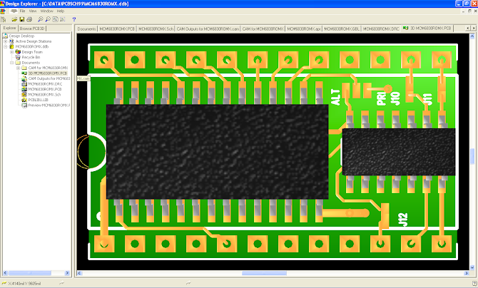
Remembering that /CS1 input is active from $E000..$FFFF, I passed CS3/A10 and CS2/A11 through to the EEPROM and added J10, J11 and J12 which are used to modify the /OE signal so it's only active for a lower range of addresses. For example if all 3 jumpers are fitted, then the /OE will only be active when all 3 are high which would be from address $FC00..$FFFF (1K). If all 3 are left open then the 3 pull-up resistors R10, R11 and R12 along with the /CS1 input signal will enable /OE for the whole 8K from $E000..$FFFF (8K). That also means CS0/A12 would need to be passed through to A12 on the EEPROM and the PRI jumper would allow that to happen.
That adds the extra feature I wanted, but to keep the original project goal (and not move the goal posts) I still need to have A12 on the EEPROM side be either high or low regardless of A12 input, and the EEPROM enabled during access to the upper 1K. That's why I have added the PRI/ALT jumper. When it's on the PRI position and J12 is connected, CS0/A12 is passed through to A12 on the EEPROM selecting the upper 4K and it also needs to be combined with A10 and A11 so the /OE is only active during access to $FC00..$FFFF. That how to select one of the two ROM options.
To select the alternate ROM version, J10, J11 and J12 still needs to be fitted, but this time A12 on the EEPROM is grounded via the ALT jumper effectively selecting the other ROM option.
So that looks good in theory and to prove that it works I re-burned my EEPROM so that I could test the 8K option. I installed the extra 3 pull-up resistors. To prevent confusion I placed the patched ROM in the upper 1K of the EEPROM from $1C00..$1FFF, and for the rest of the EEPROM was erased to #$FF, then I placed two bytes at the start of each page (256 byte boundary), so that I could check them after I installed the EEPROM and booted the ET-3400. J10, J11 and J12 were left out and CS0/A12 was passed through to A12 on the EEPROM so that the full 8K was enabled.
The memory in the EEPROM looked like this in the HxD editor:
$0100: 01 00 FF FF FF FF ...
Of course this will show up in the first 2 bytes on each page boundary from $E000, $E100, $E200 etc up to the ROM data from $FC00..$FFFF.
I installed and booted the ET-3400 successfully and checked that those page boundaries did in fact contain the edited data. New feature successful!
That worked fine so I continued with my PCB artwork. A11 and A12 and the extra resistors were added first. That seems to have been easy enough. I am just working on CS1/A12 through to A12 and this one is a bit harder to fit as it also contains extra jumper options.
BTW, the jumpers are not typical 2-pin jumpers you would normally use, instead I am just providing solder pads that can be bridged with a blob of solder. This is the only way they would fit and keep within the 24pin footprint. It's not likely that the jumpers will be altered often anyway. This project was to provide a ROM replacement with selectable alternate ROM. Anything extra is a bonus.
And now that I added the 8K option I also need to think about reprogramming the EEPROM. That's out of the scope of this project but I am taking steps in this design to at least allow it to happen later on. That's why I have added a jumper pad for the /WE signal. You need to get at that for reprogramming.
Comments
Post a Comment