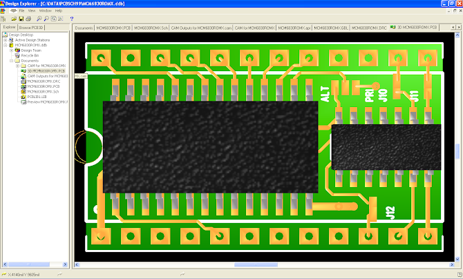
ET-3400 ROM - Draft PCB layout
I checked the data sheet for the AT28C64 and there are some write waveforms shown as below. If I want to ever have a chance of making a programming adapter board then certain pins in the original circuit have to be disconnected from a permanent connection that I had for a read only operation. The 4 pins that need to be accessible to the EPROM programmer are /CE, /OE, RDY/BUSY, and /WE. I had forgotten /OE previously. So these pins need a way to be disconnected from their read circuit. The rest of the pins needed are accessible on the edges on the 24-pin socket. I'll probably be using SIL machine pins as the ROM pins to plug this into the ET-3400 motherboard.
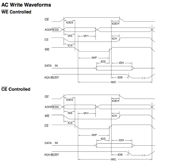
As can be seen in the above waveforms, an EPROM programmer could write to the EEPROM in a couple of ways, and both involve setting /WE, /CE and /OE high or low during the write cycle. If they are tied high or low in my original read only setup then the programmer could be damaged and it's unlikely that the EEPROM could be written either.
I've added jumper pads for all 4 of these tracks like I did for the 1K/8K selection options. All the programming options had to be moved to the bottom side of the PCB for space reasons so there are more vias now.
Thinking ahead I wanted a way to access those 4 connection points and while I don't have a full solution yet, I found some pins that may be useful. They are called pogo pins and come in a variety of types. Maybe others are familiar with them, but I've only seen them recently. I'll order some so I can design a programming board later on.

My idea is that a programming board would connect the extra pins via these pogo pins when the ROM PCB is plugged into a programming adapter, that in-turn plugs into the EPROM programmer. To make my job easier later I decided to position all the pogo pin pad connection points on a 0.1" grid so they will be easier to design a PCB for.
This is the draft PCB layout completed finally. There was a lot of manipulating required to squeeze it all in.

The grey horizontal and vertical lines were to help me position where I wanted to place pads for future pogo pin connections. Green traces are top layer and pink traces are bottom layer.
While squeezing it all in I had to swap around some of the NAND gate inputs. It won't affect the circuit operation as the sequence of inputs into a NAND gate is irrelevant. I'll have to fix up the schematic as well to match.
My next task is to do a 100% manual check of the PCB layout with the schematic (once it's patched). I'll go back to my old trusted method of printing it out on a large A3 printout and get a pencil to mark off each track on both drawings one at time. That method has served me well in the past. I didn't use this method on my last PCB that I had made and that led to at least one error that I have to manually fix on 100 tiny boards. ouch!...
Comments
Post a Comment